Food, safe house and dress are the basics that are significant for a person to dwell. With the movement of time, the example of these urgent necessities keeps changing according to any similarity to individuals. Among these the Folks Are Choosing a Custom Made Hoodie for Shufflers most unique and trendier thing is clothing. Clothing is the most compelling thing which changes reliably according to any similarity to individuals. And besides in a short period of time. There are many plans introduced by individuals for the attire styles among. Which hoodies are the most revered and mentioned dress style of people especially folks.
Cap Like Sewing
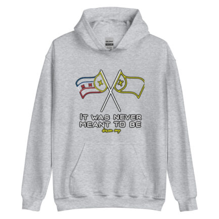
The hoodie is the latest example which is picked by folks of late. The hoodie is a sort of shirt which has a cap like sewing joined to it at the top and it comes for both energetic as well as grown-up folks. A hand created hoodie is one which is made by any similarity to the wearer and is mentioned early on thusly figuring out the requirements of the purchaser. It goes with speed for straightforward wearing and likeness of the singular wearing it. The folks are mentioning the hand created hoodie an as best wearing thing lately.
Tremendous Extension for their work
Shufflers demand the hoodie for a tremendous extension for their work. You can see a shuffler ceaselessly wearing a hoodie during playing DJ music and improving mp3s in capacities. Folks by and by favor a uniquely planned hoodie for shufflers to hard style clothing. The hard style clothing is nothing, but the style of the shufflers to uncover them more blazing than various folks in the regions. Where they play their music and the uniquely planned hoodie are magnificent to parade their goodness. And their appearance more wonderful and not exactly equivalent to the others.
Extraordinarily Planned Hoodie
The extraordinarily planned hoodie for shufflers to hard style clothing suit their lifestyle and the shoes that they wore. With the new development and the rising being involved by the shufflers for the exceptionally planned hoodies, tit is ending up being more popular among the normal people and is hugely mentioned by the male people https://ericemanuelshop.com/from one side of the planet to the next. To be sure, even the hoodies for both little youth and for adults in their sizes and they are generally mentioned by young people as they are more style aware than the children and man.
Perfect Gift for Special Occasion
In the new age various youngsters are fun of tweaking their stuff. One in line is their clothing. Many will generally show its imagination in making arrangements. In clothing an enormous part of them like hoodies, as they use for plan or consistency. Hoodies explicitly are routinely use for skaters. This will be their image name in clothing. They simply contrast from plan and style for their own choice. Changed hoodies comes in very well-known nowadays. It gives off an impression of being that a lot of web-based associations are by and by enduring requests for making innovative, redid custom hoodies and sweatshirts.
Hoodies in no Doubt Sensible rate
Right when you endeavor to visit a part of this site you will sort out how they are wonderful to make a changed hoodies in no doubt sensible rate. Associations are very delicate when it comes in making this solicitation in light of the fact that for them having extraordinary thing making extraordinary result in their business. Custom hoodies are ordinarily use for winter to keep you warm and for others they use it for plan. This can be worn by any direction however lengthy it fit and by choice.
Particular Impact
The particular impact could be absolutely popular as well as capable that engage it to arrange the objective including connecting with the arranged watchers really. The associations ought to know your decision and make available with the arrangement for the hoodie that you expected to re-try. Having your own arrangement and method of attire makes you satisfied as you wear your own imaginative work unlike others.
Truly Brilliant and Significantly
Since people right now are altogether famous, they endeavoring to make something different, different that you simply have your own arrangement. A certified model for this is the place where you expect to give a novel gift for your love once. In all likelihood, you will expect to make something unique that maybe the one gets it will surely esteem and feel an obligation of appreciation much. In arranging guarantee that it will go with the choice of the wearer. It absolutely is truly brilliant and significantly greater for them.